류형록 | Engineering Portfolio · 전체 프로젝트
<aside> 📌
KiCad 2층 PCB / SFH7070 ×2·OPA2333 ×3·STM32F411
69 modules · 83 nets · 602 tracks · Gerber·drill
</aside>
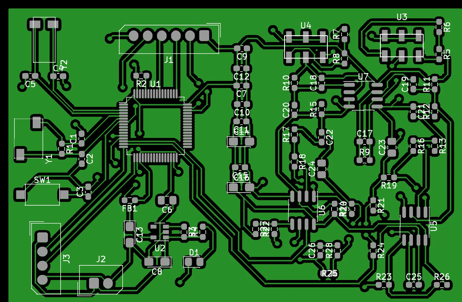
STM32F411 PPG PCB front view
산출물: KiCad 회로도·PCB·Gerber·drill
I designed a two-layer PPG PCB integrating two SFH7070 optical sensors, three dual OPA2333 zero-drift amplifiers, and an STM32F411RETx. The project connects the analog front end to ADC inputs A0/A1 and carries the design through KiCad routing, ground copper, Gerber, and drill outputs.
SFH7070 ×2 → OPA2333 amplification/filter stages → STM32F411 ADC A0/A1 → digital processing/UART
5 V input → SPX3819 3.3 V rail → analog/digital circuits